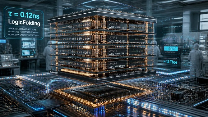
The semiconductor industry has a problem, and it’s not just about shrinking transistors anymore. For decades, Moore’s Law served as the industry’s guiding star—double the transistors every two years, and performance follows. But the physical limits are real, and for companies cut off from the most advanced manufacturing tools, the challenge is existential. At this year’s IEEE International Symposium on Circuits and Systems in Shanghai, Huawei proposed a fundamentally different answer. Instead of asking how small a transistor can be made, they asked how fast information can move through a chip. That shift in thinking—from geometric scaling to time scaling—represents one of the most consequential semiconductor strategy pivots in recent memory.
The Tau Scaling Law: A New Physics for Semiconductors
Huawei’s response is the Tau (τ) Scaling Law, presented by He Tingbo, President of Huawei’s Semiconductor Business. Named after the Greek letter for time constant, τ scaling replaces geometric miniaturization with the compression of signal propagation delay at every level of the chip’s architecture. The core idea is deceptively simple: performance isn’t determined by how many transistors you can pack into a square millimeter, but by how quickly signals can traverse the chip’s circuits. By reducing τ—the time it takes for electrical signals to move through the system—Huawei can deliver better performance without needing to shrink transistors to ever-more-advanced process nodes.
The practical implementation of this theory is an architecture called LogicFolding. Rather than laying circuits flat on a single silicon plane, LogicFolding stacks active logic circuits vertically, like adding floors to a building. This is not simply 3D memory stacking like HBM; LogicFolding distributes registers, digital logic, and analog circuits across multiple wafer layers connected by hybrid bonding and vertical interconnects. The result? Signal paths that once traversed long metal traces across a chip are now reduced to short vertical channels between layers. It’s like converting a sprawling single-story factory into a multi-floor facility—processing power increases without expanding the footprint.
The Numbers That Matter
The performance claims are staggering. Using identical manufacturing processes as the 2025 Kirin 9030 Pro baseline, the LogicFolding-equipped Kirin 2026 chip achieves transistor density of 238 MTr/mm² under Huawei’s measurement methodology, which translates to approximately 175.4 MTr/mm² by industry standard—slightly exceeding TSMC’s 5nm planar process standard logic density range of 138-171 MTr/mm². This represents a single-iteration density improvement that would traditionally require three years of geometric scaling to achieve.
Equally impressive: the Kirin 2026 reduces supply voltage by 0.2V while maintaining equivalent performance to its predecessor, with measured power consumption at only 59% of the baseline and power density at 94.4%. That’s a 41% improvement in power efficiency through architectural innovation alone. And Huawei emphasizes this is a conservative implementation—they project transistor density could reach 400 MTr/mm² or higher by 2035, with Kirin CPU core frequencies exceeding 4 GHz.
Beyond Mobile: Implications for AI and Data Centers
The significance of Tau Scaling extends well beyond smartphones. Huawei’s Ascend chip series already sits at the center of China’s domestic AI computing stack, powering models including DeepSeek’s latest. If LogicFolding delivers on its performance claims as it rolls out across the Ascend line through 2027 and 2028, the gap between Chinese AI hardware and Nvidia’s best-in-class offerings could close considerably.
For AI data centers, the implications are particularly acute. Over 80% of energy in AI systems is consumed by data transfer, and over 70% of system cost goes to data storage. Huawei’s data center implementation employs a Unified Bus architecture, the Hi-ONE near-package optical engine, and 3D Folding packaging topology to compress communication time constants at the system level. By 2031, Huawei projects its high-end chips will match the transistor density of a 1.4-nanometer process—the level TSMC is targeting for 2028. The gap is now measured in years, not decades.
Industry Validation and Real-World Impact
The industry is taking notice. At MWC Barcelona 2026, Huawei won eight prestigious GLOMO Awards, including Best Mobile Network Infrastructure and Best AI-Powered Network Solution. The company has mass-produced 381 chips designed under the τ Scaling Law between May 2020 and May 2026, across a wide range of products and industries.
In enterprise storage, Gartner recognized Huawei as a Leader in its 2026 Magic Quadrant for Enterprise Storage Platforms—the only non-North American vendor to earn that position. The OceanStor Data Storage portfolio leverages a high-efficiency, unified AI data platform with excellent capacity density and energy efficiency.
The Road Ahead: Challenges and Open Questions
Huawei’s path is not without challenges. The company acknowledges that significant hurdles remain, including toolchain and methodology development, managing wafer-to-wafer process variation, and overcoming vertical interconnect overhead. The sheer complexity of stacking multiple active layers—with thermal budgets between layers and through-silicon vias that must be carefully managed—presents engineering challenges that no single company can solve alone.
He Tingbo’s presentation positioned the work as both a field report and an invitation to the broader industry. “We believe that openness and collaboration are key to driving ongoing progress in the semiconductor industry,” she noted. It’s a diplomatic stance that also reflects practical necessity: the toolchains, design methodologies, and manufacturing processes for 3D-stacked chips are still nascent, and Huawei cannot build them in isolation.
A Different Kind of Scaling
What makes Huawei’s achievement noteworthy isn’t that LogicFolding and chip stacking are entirely new concepts—TSMC, Samsung, and Nvidia have all invested in similar approaches. The difference is context. Huawei is attempting to design and mass-produce these chips using a largely domestic supply chain, under the constraint of advanced lithography equipment bans. Rather than waiting for the conventional path to open up, they’ve built a different one.
The Tau Scaling Law represents a philosophical shift in how we think about semiconductor progress. In the post-Moore era, performance gains will come not just from manufacturing process improvements but from architectural innovation, advanced packaging, and system-level optimization. Huawei’s 381 mass-produced chips are proof that this approach can work at commercial scale.
Whether all of the projected performance targets are achieved remains to be seen. But the direction is clear: the future of semiconductor innovation is no longer solely determined by how small we can make transistors, but by how cleverly we can arrange them.